
Pixel change detection camera
OV5640 camera + iCE40UP5K FPGA frame-difference + ESP32-S3 Wi-Fi + ASM330LHH IMU, powered from USB-C (no coin cell).
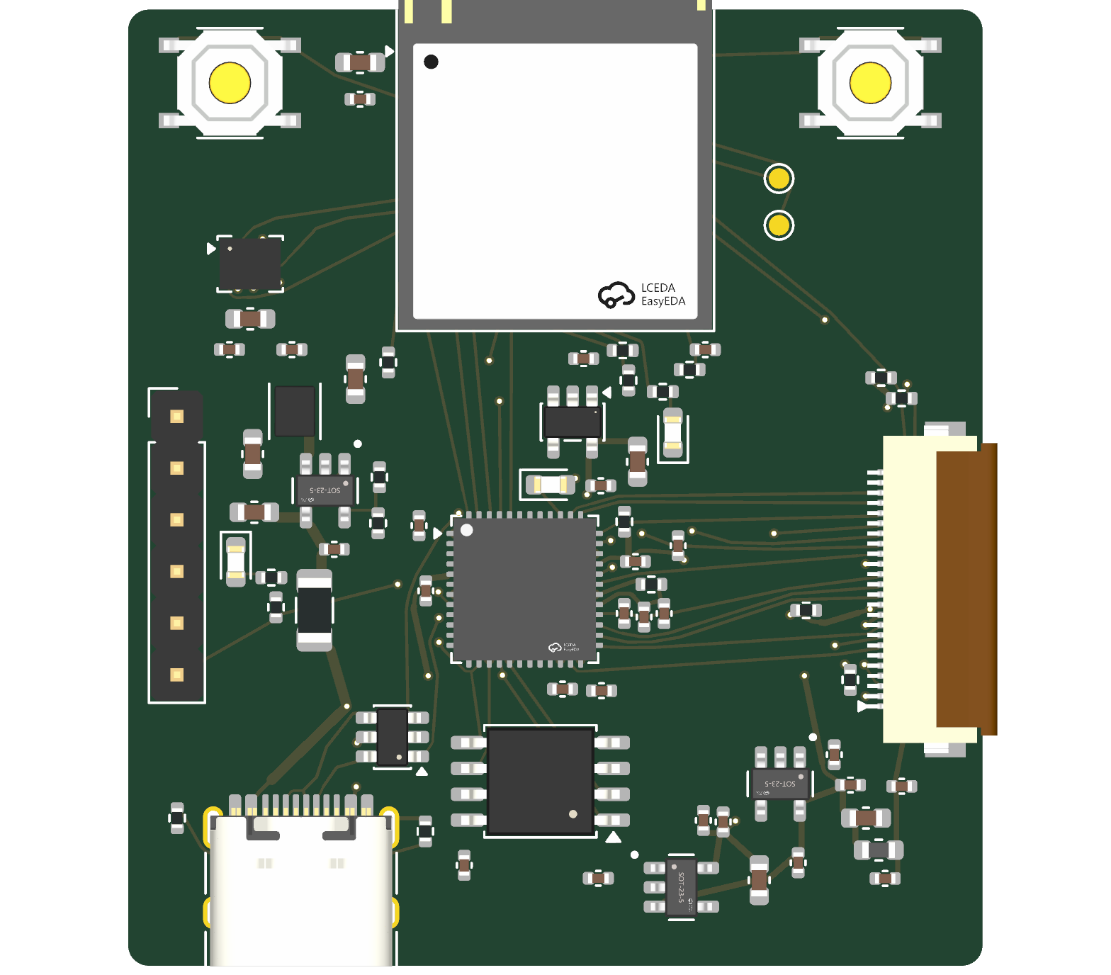
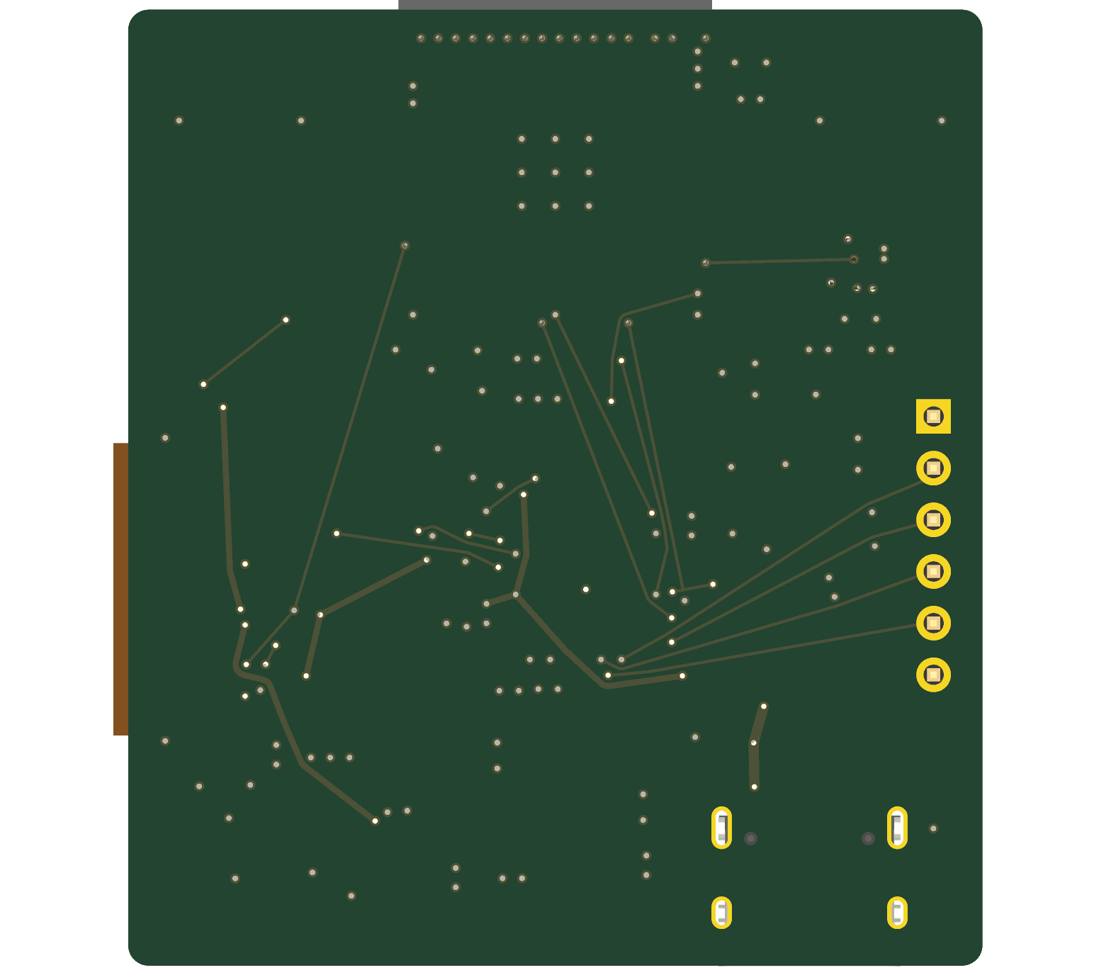
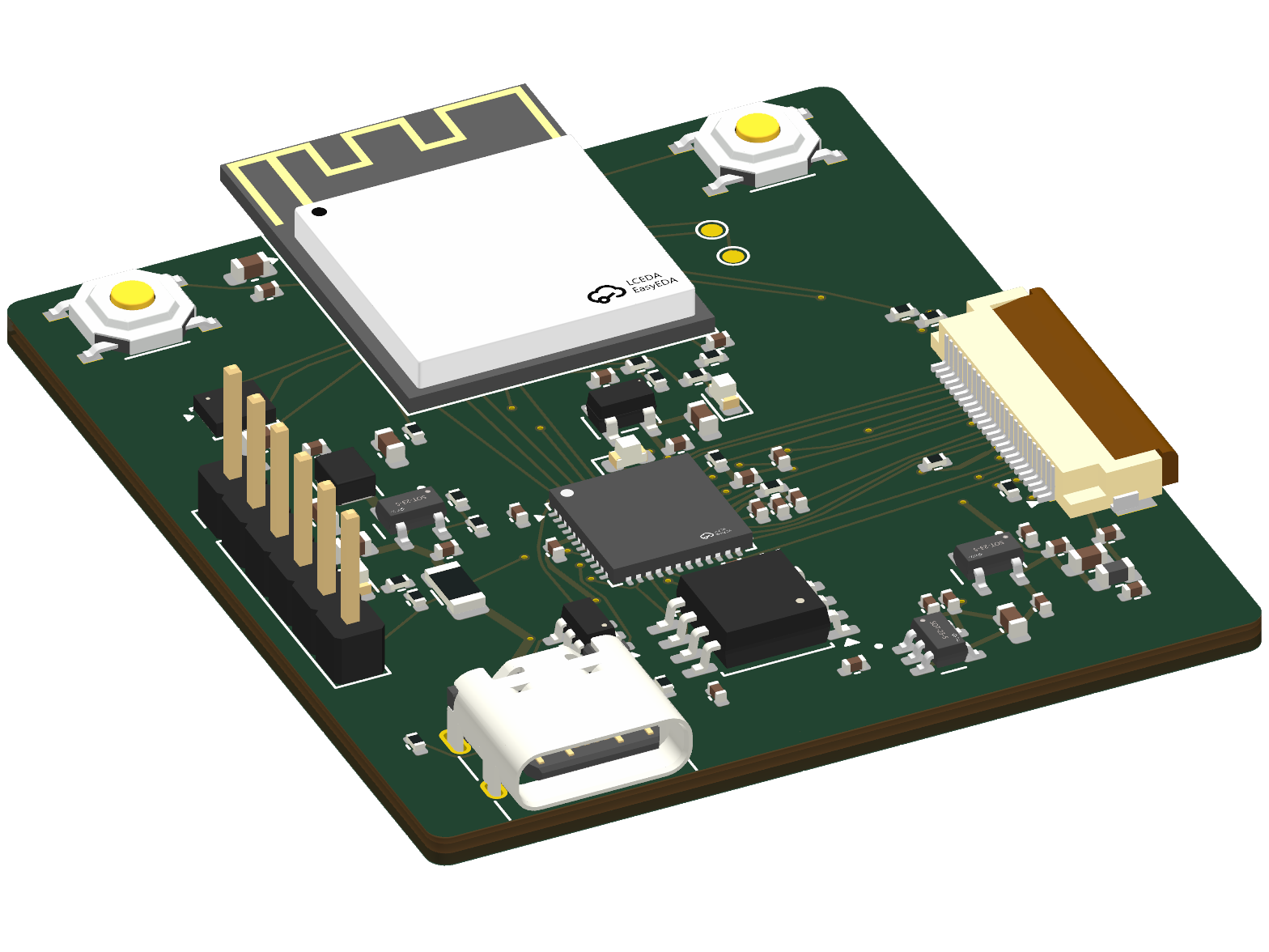
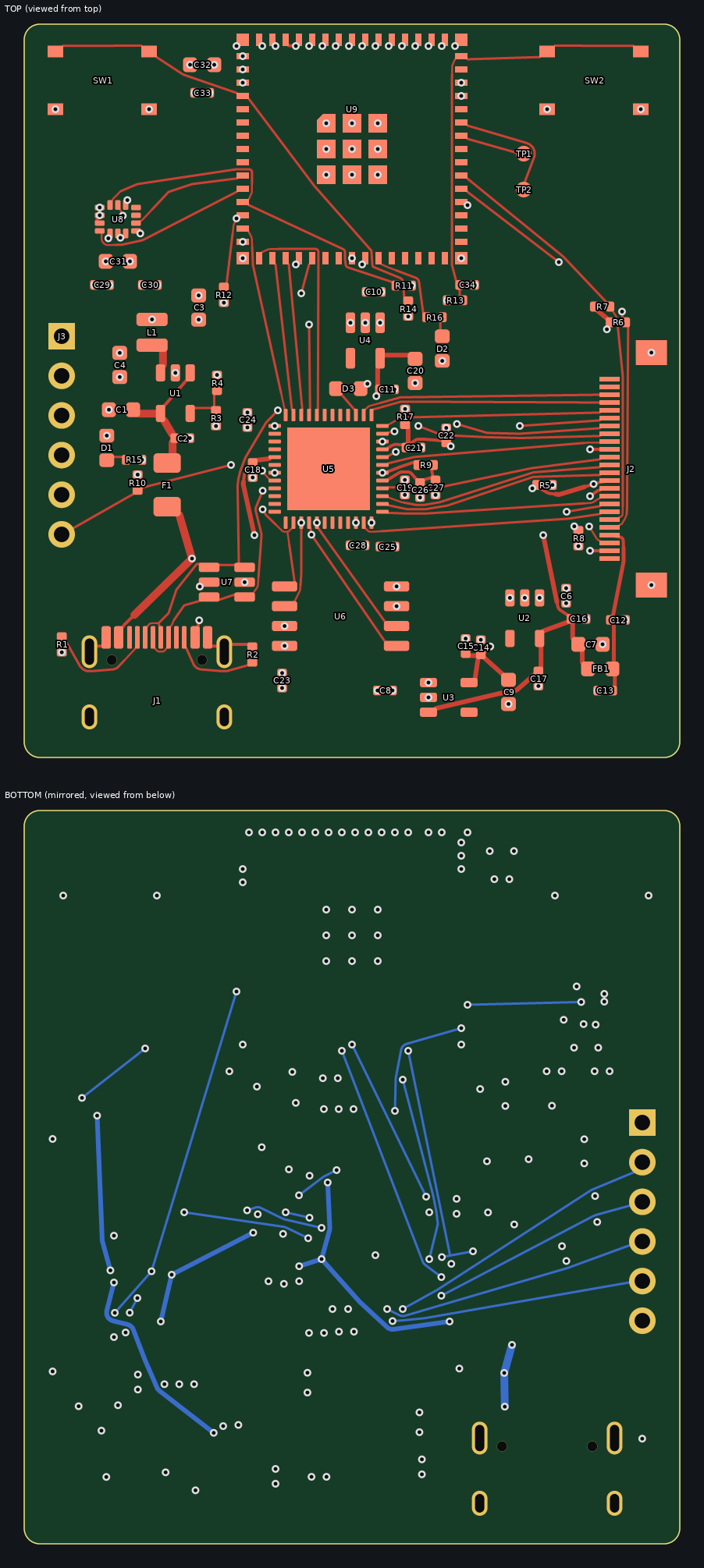
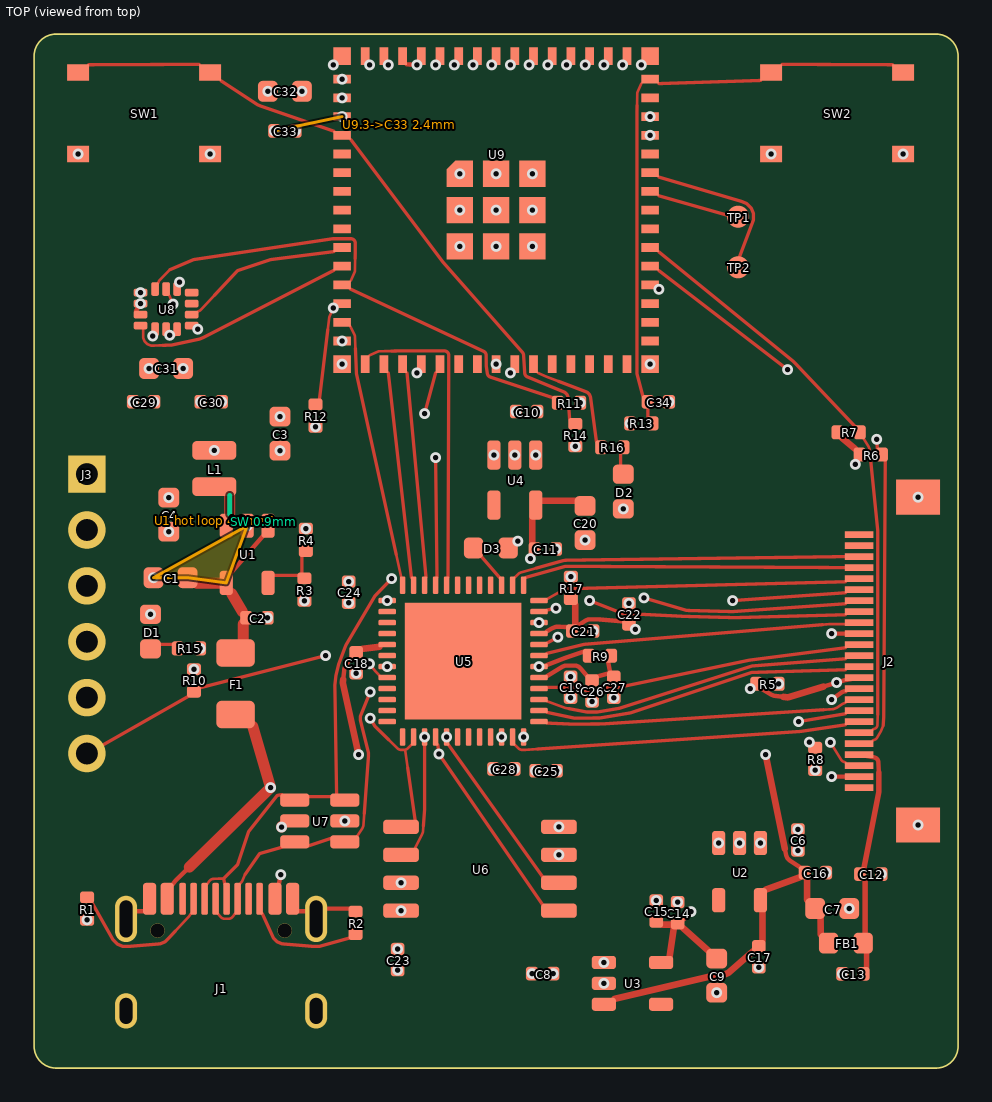
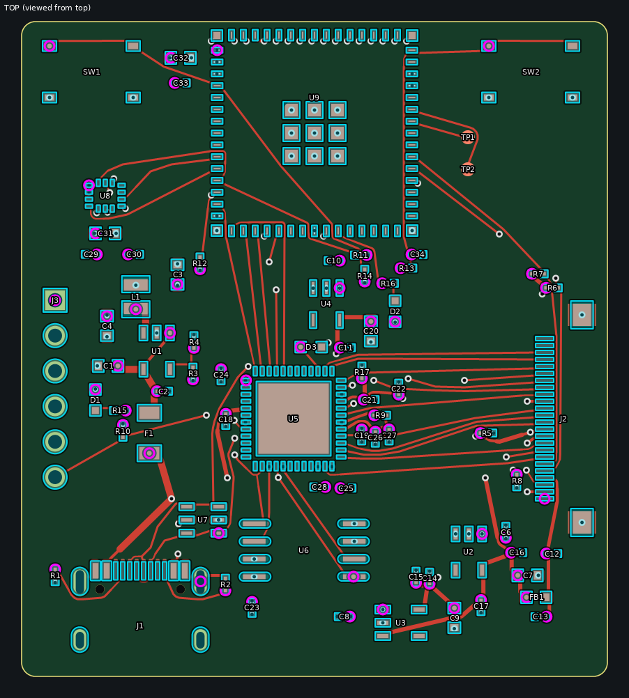
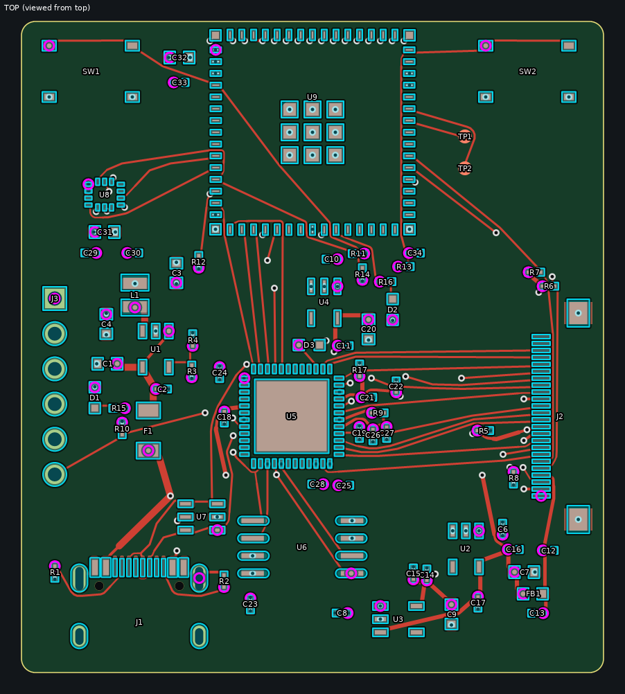
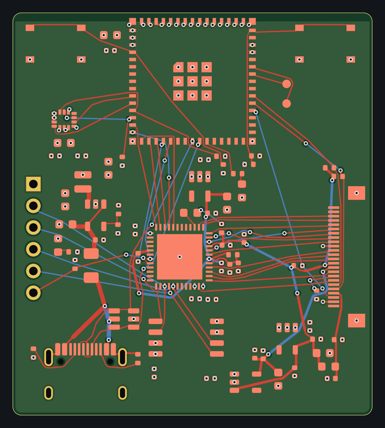
| OK | verc (voltage domains, power, thermal) VERC_OK (0 warning(s)) |
| Warning | datasheets + part rules SPECCHECK_WARN: 12 warning(s), 11 rule(s) checked |
| OK | netaudit (graph = schematic = pcb) NETAUDIT_OK (0 warning(s)) |
| OK | KiCad DRC DRC_OK |
| OK | power loops + decoupling LOOPS_OK: 0 error(s), 3 warning(s) |
| OK | placement rules PLACE_OK: 13 of 45 placement rules outside limits, 5 review finding(s) (warnings); anchors: run/out/place_anchors.png |
| OK | JLC CPL emulation CPL_OK |
| OK | JLC stock (3 boards) STOCK_OK |
| OK | 3D models (warning only) MODELS3D_OK: all 70 parts with a body have a 3D model (2 without one by design: TP1, TP2) |
| OK | render |
- 3D model (glTF)board.glb · 448.5 KB
- Render, toprender_top.png · 130.9 KB
- Render, bottomrender_bottom.png · 84.1 KB
- Render, isometricrender_iso.png · 326.9 KB
- Schematic (PDF)schematic.pdf · 339.9 KB
- Gerbers + drill for JLCPCBgerbers_jlcpcb.zip · 110.0 KB
- BOM for JLCPCB assemblybom_jlc.csv · 1.6 KB
- Full BOMbom_full.csv · 2.2 KB
- Pick & place (CPL)cpl_jlc.csv · 2.7 KB
- Verification summarycheck_summary.jsonl · 971 B
- Electrical review (voltage domains, power, thermal)verc_report.md · 18.7 KB
- JLC stock checkstock_check.txt · 3.0 KB
- Placement reviewplace_rules.md · 5.8 KB
Design your own board
Describe a circuit in plain words. An AI engineer takes it to order-ready files.